McGill University
ECSE 534
THREE-STAGE CMOS OPERATIONAL TRANSCONDUCTANCE AMPLIFIER
Assignment # 2
Arun Arun 260881882
M.Eng. Student, McGill University
Arun.butte@mail.mcgill.ca
Abstract—Three stage OTA is presented in this paper where the first stage is a differential input stage and to increase the gain, two additional common source stages are added. This is impleme
...[Show More]
THREE-STAGE CMOS OPERATIONAL TRANSCONDUCTANCE AMPLIFIER
Assignment # 2
Arun Arun 260881882
M.Eng. Student, McGill University
Arun.butte@mail.mcgill.ca
Abstract—Three stage OTA is presented in this paper where the first stage is a differential input stage and to increase the gain, two additional common source stages are added. This is implemented in 65nm technology in cadence. This OTA has a supply of 1v and all the transistors in the circuit as biased such that they are in saturation to achieve a gain of approximately 67dB with static power consumption of 41µA.
Keywords—Three stage, OTA, gain, power consumption.
I. INTRODUCTION
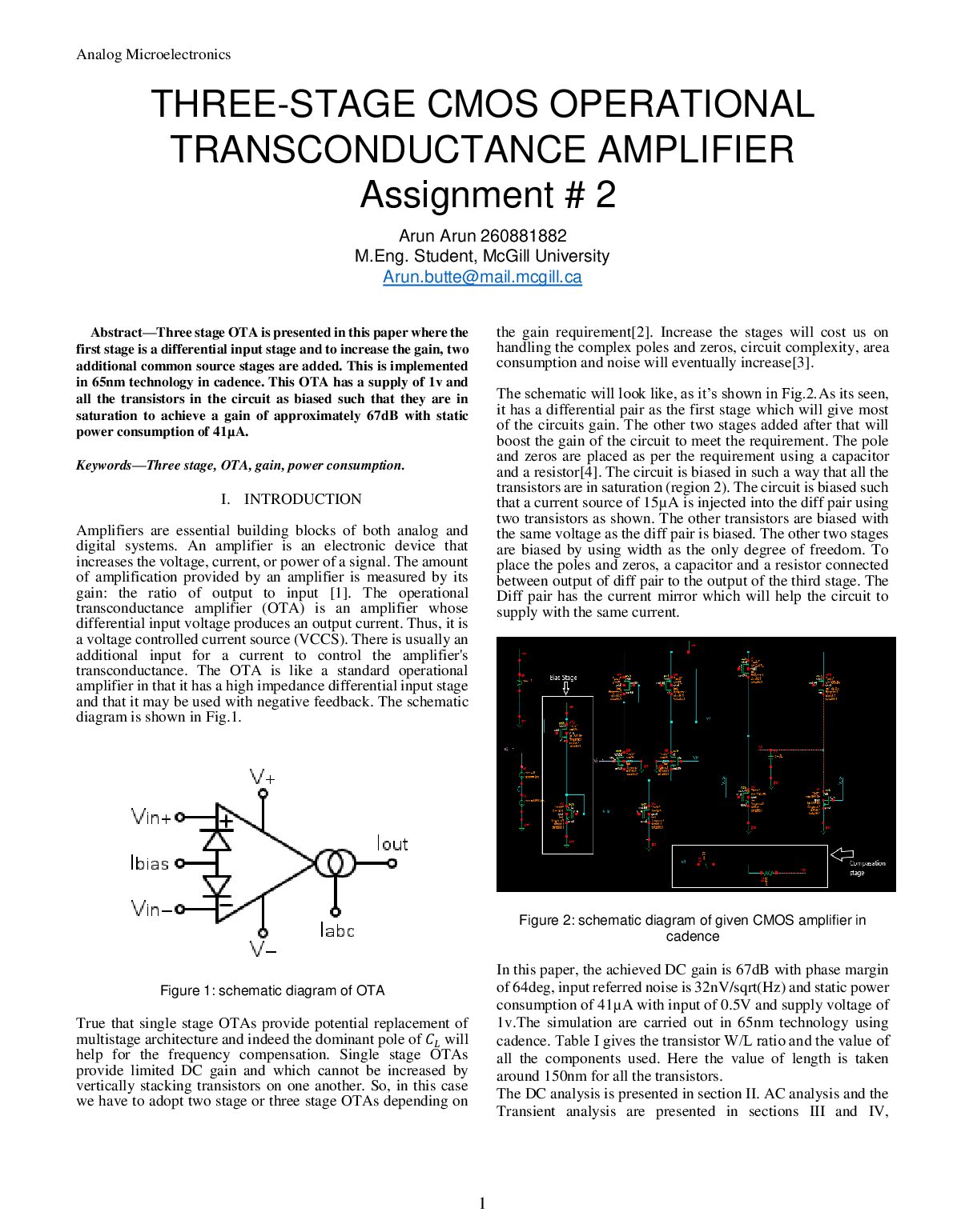
Amplifiers are essential building blocks of both analog and digital systems. An amplifier is an electronic device that increases the voltage, current, or power of a signal. The amount of amplification provided by an amplifier is measured by its gain: the ratio of output to input [1]. The operational transconductance amplifier (OTA) is an amplifier whose differential input voltage produces an output current. Thus, it is a voltage controlled current source (VCCS). There is usually an additional input for a current to control the amplifier's transconductance. The OTA is like a standard operational amplifier in that it has a high impedance differential input stage and that it may be used with negative feedback. The schematic diagram is shown in Fig.1.
Figure 1: schematic diagram of OTA
True that single stage OTAs provide potential replacement of multistage architecture and indeed the dominant pole of 𝐶𝐿 will help for the frequency compensation. Single stage OTAs provide limited DC gain and which cannot be increased by vertically stacking transistors on one another. So, in this case we have to adopt two stage or three stage OTAs depending on the gain requirement[2]. Increase the stages will cost us on handling the complex poles and zeros, circuit complexity, area consumption and noise will eventually increase[3].
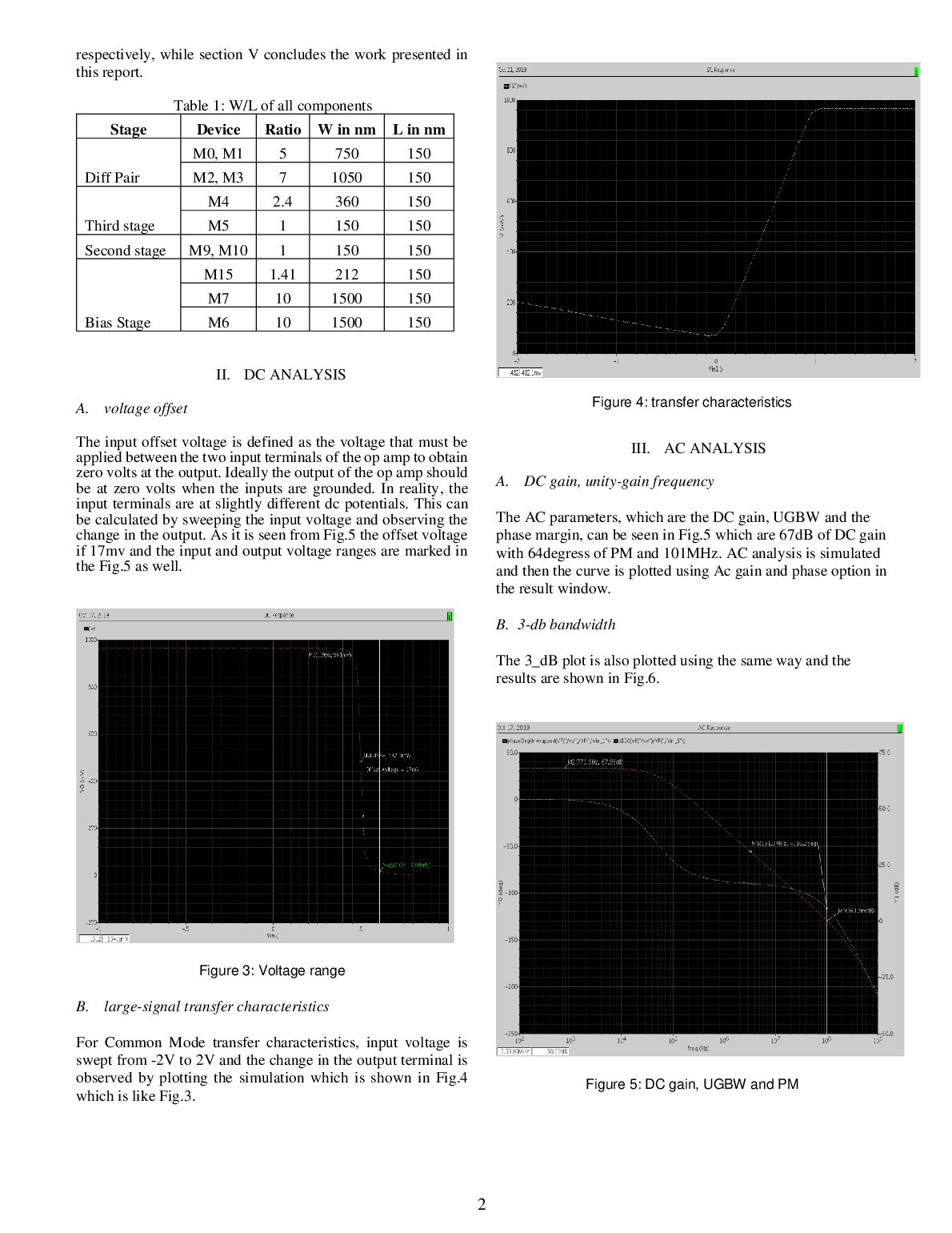
The schematic will look like, as it’s shown in Fig.2.As its seen, it has a differential pair as the first stage which will give most of the circuits gain. The other two stages added after that will boost the gain of the circuit to meet the requirement. The pole and zeros are placed as per the requirement using a capacitor and a resistor[4]. The circuit is biased in such a way that all the transistors are in saturation (region 2). The circuit is biased such that a current source of 15µA is injected into the diff pair using two transistors as shown. The other transistors are biased with the same voltage as the diff pair is biased. The other two stages are biased by using width as the only degree of freedom. To place the poles and zeros, a capacitor and a resistor connected between output of diff pair to the output of the third stage. The Diff pair has the current mirror which will help the circuit to supply with the same current.
Figure 2: schematic diagram of given CMOS amplifier in cadence
In this paper, the achieved DC gain is 67dB with phase margin of 64deg, input referred noise is 32nV/sqrt(Hz) and static power consumption of 41µA with input of 0.5V and supply voltage of 1v.The simulation are carried out in 65nm technology using cadence. Table Ⅰ gives the transistor W/L ratio and the value of all the components used. Here the value of length is taken around 150nm for all the transistors.
The DC analysis is presented in section II. AC analysis and the Transient analysis are presented in sections III and IV,
[Show Less]